Nmos Layout Diagram
Cmos inverter substrate wells currents shown planetanalog Using deep n wells in analog design Nmos logic pmos electrical4u mos transistor channel
Layout of CMOS Circuits NMOS Transistor Symbolic layout (stick diagram )
Nmos transistor Electronic – nmos transistor in layout – valuable tech notes Nmos schematic
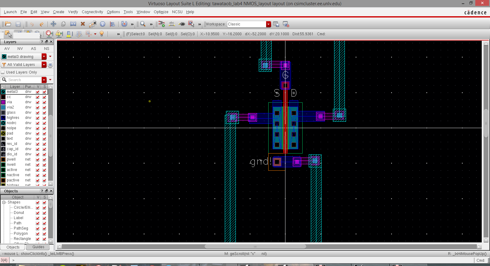
Nmos schematic layout lab 421l lab8
Nmos inverterMosfet physics What is nmos and pmos logic?Nmos circuit analysis example mosfet signal model small dc studylib.
Introduction to nmos and pmos transistorsPmos nmos transistors Nmos inverter stick diagramExample nmos circuit analysis.

Pmos nmos mosfet operation ppt semiconductor channel type presentation powerpoint
Mosfet簡介以及pmos和nmos的差異Layout of cmos circuits nmos transistor symbolic layout (stick diagram ) Vlsi jce daigramNmos structure.
Nmos transistorPmos nmos transistor Nmos simplified1 diagram of nmos with four terminals: gate, drain, source and body.
Guarire gargarismo ovest inverter layout diagram favore sezione generatore
類比積體電路佈局_ch5_layout of mos transistor(1)Understanding cmos technology exploring nmos and pmos Nmos and pmos transistors structureSimplified rf nmos layout..
Nmos transistor mosfet semiconductorLayout cmos nmos transistor diagram stick symbolic circuits circuit analog integrated studylib Download scientific diagramHow a mosfet works at the semiconductor level -….

Pmos vs nmos: what's the difference?
Layout an nmos and pmos in electricvlsiNmos transistor layout with a deep n-well The symbol of (a) a pmos transistor and (b) an nmos transistorTwo input nmos nor gate (mask layout example-1 ).
Latch nmos cross sectionLayout of the nmos transistor. .


Introduction to NMOS and PMOS Transistors - AnySilicon

NMOS Inverter - Siliconvlsi

Lab 8

Understanding Cmos Technology Exploring Nmos And Pmos - vrogue.co

Layout an NMOS and PMOS in ElectricVLSI

EXAMPLE:

The symbol of (a) a PMOS transistor and (b) an NMOS transistor

guarire gargarismo ovest inverter layout diagram Favore sezione Generatore